|
|
|
|
|

|
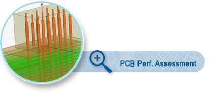
Return loss is frequently a measure of performance for high-speed interfaces. Generally it is highly sensitive to pad and antipad sizes in the PCB. Socket and connectors can therefore only unfold their potential if the PCB design is optimized for a particular component and PCB stackup. Our experience in load board and probe card design and analysis allows us to quickly and accurately predict via 3D simulation what the expected performance will be.
Moreover, using our 3D simulation toll HFSS we can readily optimize any PCB design to achieve the necessary performance.
|
|
|

